compute-in-memory AI chip · CIM · SRAM CIM · near-memory compute · MaskROM
What Is a Compute-in-Memory AI Chip? Three Routes Explained
Fanshi Semiconductor engineering team · Published
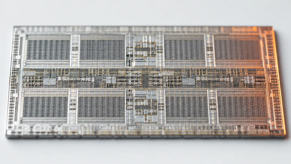
A compute-in-memory (CIM) chip performs multiply-accumulate operations inside the memory array, so model weights never leave the storage cells. It targets the largest cost in LLM inference: moving weights from memory to the compute units. By where the weights live, there are three main routes: MaskROM compute-in-memory, SRAM compute-in-memory and near-memory compute.
The problem is data movement, not compute
Every token an LLM generates requires reading all of the model's weights. For a 0.8B-parameter model at INT8, that is at least 0.8 GB read from memory per token. In a conventional architecture the data crosses a bus into the compute units and the results are written back. The arithmetic itself is a small share of the energy; most of the power and time goes into moving data.
This is the memory wall. Data centres push through it with HBM and generous power budgets. Edge devices cannot: their memory bandwidth is in the tens of GB/s and their power budget is a few watts. As long as weights have to move, an edge device cannot run a capable LLM.
Compute-in-memory turns the problem around. If moving weights is the bottleneck, stop moving them. The weights stay in the memory array, multiply-accumulate circuits sit inside or right next to it, activations flow in and results flow out.
Three routes, defined by where the weights live
MaskROM compute-in-memory: the weights are physically cast into a via array in the silicon at the mask stage of tape-out. The array is read-only and there is no external weight movement at runtime, which gives the lowest power and the lowest marginal cost per inference. The trade-off is a fixed model: changing it means new masks. It suits stable models shipping at volume, such as handheld translators and offline voice assistants.
SRAM compute-in-memory (SRAM CIM): multiply-accumulate happens inside the SRAM array, and the weights are loaded at power-up, so they can be updated. Computation still never leaves the storage cells, but the model can be swapped in the field. It suits mid-size models and products that keep iterating.
Near-memory compute: the weights reside in high-bandwidth external memory, the compute units sit right next to it, and on-chip streaming keeps movement to a minimum. It is not strictly in-memory, but for large models that are still evolving quickly it is the most practical choice.
How to choose: first ask how often the model changes
The first question is not compute but update cadence. If the model will not change for a year and you are shipping hundreds of thousands of units, nothing beats MaskROM on cost and power. If the model is revised every quarter, near-memory compute or SRAM CIM is the safer choice.
The second question is parameter count. A sub-watt power budget corresponds to models of roughly 1B parameters or less. Running a 30B-class model at the edge takes the near-memory route and a system budget of tens of watts.
Fanshi Semiconductor's first-generation chips map onto the three routes. Forge uses MaskROM for sub-watt devices running Qwen 3.5 0.8B. Trident uses near-memory compute and supports up to Qwen 3.5 35B. Argus uses SRAM compute-in-memory for 120 FPS real-time vision. All figures are design targets.
Common misconceptions
"Compute-in-memory needs an advanced process node." It does not. The gain comes from the architecture, not from transistor density. Fanshi builds on a mature SMIC 28 nm supply chain, which is also what keeps cost and supply predictable.
"Compute-in-memory can only run small models." The MaskROM route does favour fixed small and mid-size models, but the near-memory route carries tens of billions of parameters. The real limit is the power budget, not the architecture.
"Accuracy suffers." Digital compute-in-memory, unlike early analog in-memory computing, performs exact integer multiply-accumulate in the array. Accuracy is set by the quantization scheme, exactly as it is for INT8 inference on a GPU.