model-on-chip · hardwired LLM chip · model-specific ASIC · Taalas HC1 · edge LLM chip
Model-on-Chip Explained: Hardwired LLM ASICs, Cloud vs Edge
Fanshi Semiconductor engineering team · Published · Updated
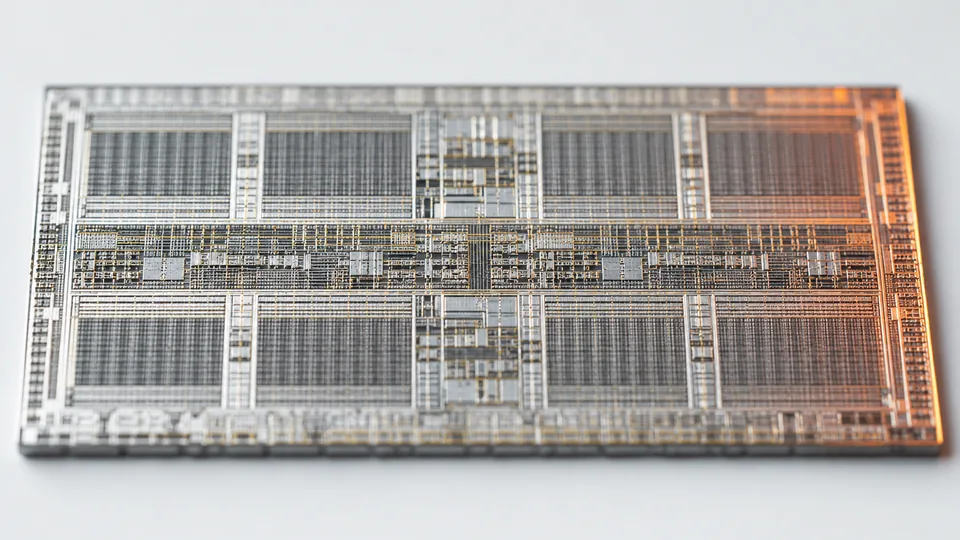
A model-specific ASIC, sometimes called a hardwired LLM chip, fixes the weights of one large language model into the silicon at manufacture. Inference no longer moves weights out of memory, so decode speed and energy efficiency can be orders of magnitude better than a general-purpose GPU. The trade-off is that the model cannot be swapped freely. There are two kinds: cloud chips chase tokens per second per rack and cost per token, while edge chips chase watt-level power, offline operation and device cost.
What "hardwired" actually means
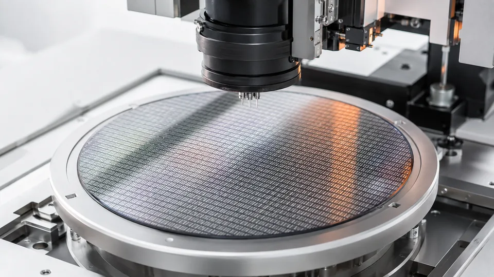
A general-purpose GPU is a machine that can run any model: the weights sit in memory and are read once for every token generated. A model-specific ASIC does the opposite. The model is chosen at design time and its weights are written into mask ROM or metal layers, so they become part of the chip. When the chip leaves the fab, the model is already inside.
What this removes is the most expensive step in inference: moving the weights. The compute units stop waiting for data, bandwidth stops being the ceiling, and most of the power is no longer spent in transit.
Why this is happening now
Two things turned the idea into products. First, model families have become structurally stable: a newer release often keeps the layer layout of the previous one, so a chip architecture built for one model can carry over to the next. Second, inference bills keep growing. Per-token pricing and the cost of power both push the industry to build dedicated hardware for the handful of models that are used the most.
It does not replace the GPU. Training, research and long-tail models still need general-purpose hardware. A model-specific ASIC fits where the model is settled and the volume is very large, or the power budget is very tight.
Cloud and edge have different goals
A cloud chip of this kind lives in a data centre and is measured against GPU servers: tokens per second per rack and dollars per million tokens. It usually uses a more advanced process node and draws hundreds of watts.
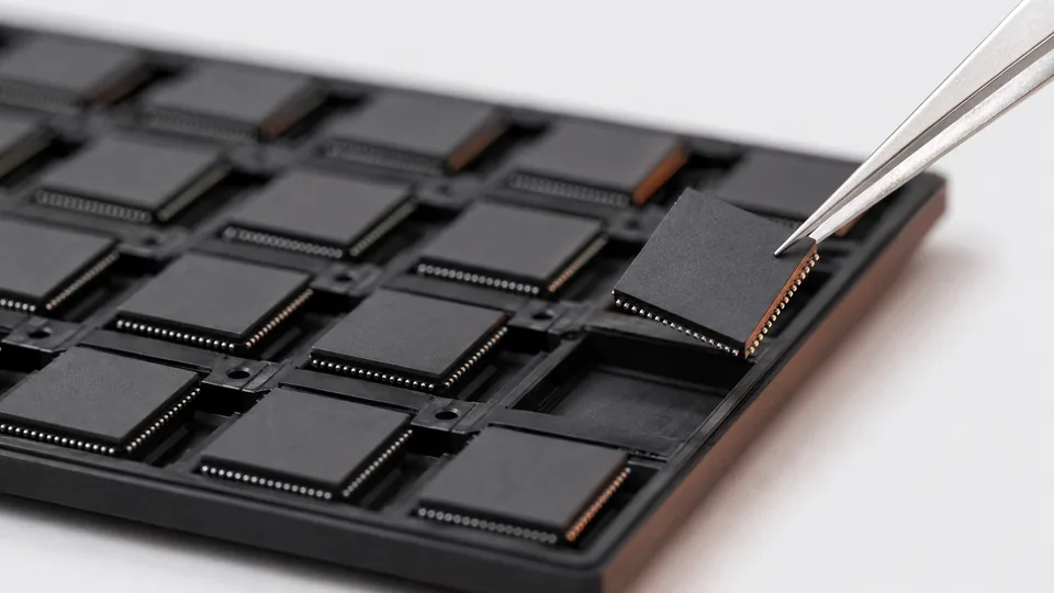
An edge chip lives inside a device: a translator, a car, a robot, an industrial camera. The questions are whether it runs in one watt to a few tens of watts, whether it works without a network, and how much it adds to the bill of materials. Data never leaves the device, which is a hard requirement in air-gapped and privacy-sensitive deployments.
Fanshi Semiconductor builds the edge kind. On a mature SMIC 28 nm supply chain it offers three routes, MaskROM compute-in-memory, SRAM compute-in-memory and near-memory compute, covering watt-class handhelds up to heavy-load nodes that run 35B models. All figures on the site are design targets.
The public reference point: Taalas HC1
The clearest public example is the Taalas HC1, announced in February 2026. According to the company and press coverage, it hardwires Llama 3.1 8B into a single ASIC of about 53 billion transistors, made on TSMC 6 nm with an 815 mm² die, and generates close to 17,000 tokens per second per user. For the same model the coverage cites roughly 230 tokens per second on an NVIDIA H200 and about 1,900 on Cerebras in independent benchmarks.
Two details matter for anyone evaluating the approach. By the company's own account the first silicon is aggressively quantized, combining 3-bit and 6-bit parameters, which costs some answer quality against a GPU baseline. And it is a data-centre product, designed for servers of around 2.5 kW, not something that fits inside a device.
The edge variant applies the same idea, weights that never move, on a mature process node to models sized for one watt to a few tens of watts.
What to ask a vendor
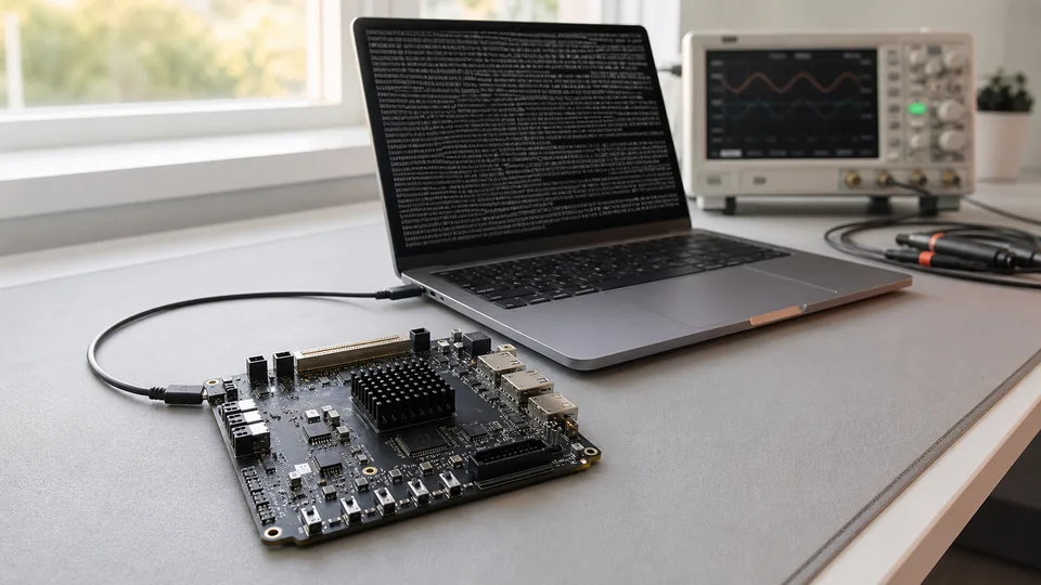
First, what happens when the model changes: new masks, a reload, or an update to external memory? Can a newer model in the same family reuse the existing architecture? Second, are the published figures measured or design targets, and for which model, precision and test conditions? Third, can you get an evaluation board before tape-out and run your own model and data on it? Fourth, how predictable are the process and the supply chain, and what sets the delivery schedule?
If you are evaluating this kind of chip for a device, the project brief page on the Fanshi site takes two minutes: describe the model, the device, the power budget and the volume, and the engineering team replies about your project.
Frequently asked questions
Can the model in a hardwired chip be updated?
It depends on where the weights live. With mask ROM the weights are part of the mask set, so a new model means new masks; some designs still allow adapter-style adjustments and a configurable context window. With SRAM compute-in-memory the weights are loaded at power-up and can be replaced. With near-memory compute they sit in external memory and can be updated like firmware.
Is model-on-chip the same as compute-in-memory?
They overlap but are not the same. Model-on-chip describes the product decision: one model is fixed into the silicon. Compute-in-memory describes the circuit technique: arithmetic happens inside the memory array. A mask-ROM chip that computes in the array is both; an SRAM compute-in-memory chip is compute-in-memory without a fixed model.
How fast is a hardwired LLM chip?
The public reference is the Taalas HC1, reported by the company at close to 17,000 tokens per second per user on Llama 3.1 8B. That is a vendor figure for one model at one quantization. For any chip, ask whether a number is measured or a design target, and for which model and precision.
Is Fanshi related to Taalas?
No. Fanshi Semiconductor has no affiliation or partnership with Taalas. The two companies share a broad technical direction; Taalas builds data-centre accelerators, Fanshi builds chips and IP for edge devices.