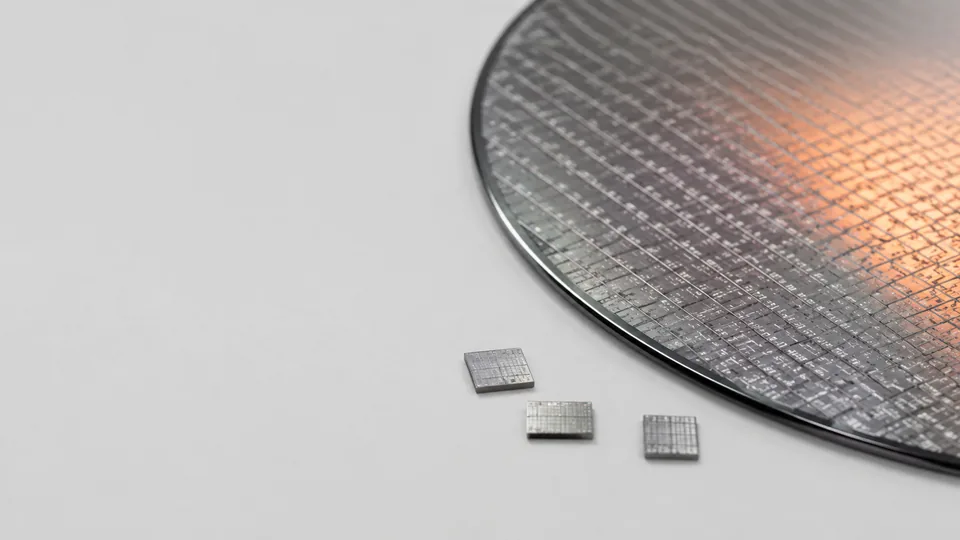
FPGA prototyping for LLM accelerators · LLM inference IP · semiconductor IP licensing · FPGA LLM · ASIC tape-out
FPGA Prototyping for LLM Accelerators: IP Licence to Tape-out
Fanshi Semiconductor engineering team · Published
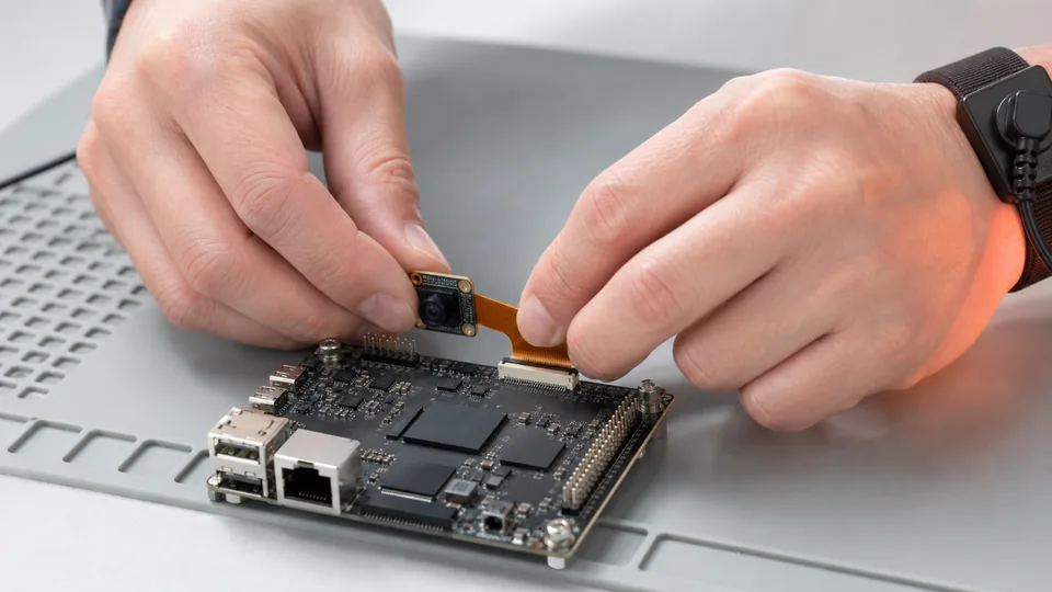
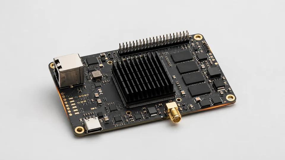
FPGA prototyping for LLMs means deploying an inference core IP on an FPGA evaluation board before tape-out and running the full path with a real model and real interfaces. It puts an engineering sample in your hands before the ASIC exists, exposes model-mapping, quantization-accuracy, interface and integration issues early, and gives the tape-out decision measured evidence.
Why start on an FPGA
An ASIC tape-out is slow and expensive; one mistake costs months and a significant sum. An FPGA can run the same inference core within days and validate it with a real model, real interfaces and real data. Is the model mapping right? How much accuracy does quantization cost? Is the interface bandwidth sufficient? How does the system software connect?
For product teams, the FPGA evaluation board is the first engineering sample. It can go into user testing, customer demonstrations and field data collection while the ASIC is still being designed.
What an inference IP licence includes
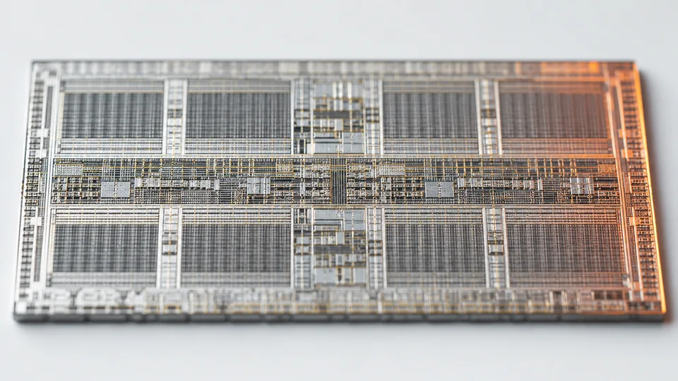
Fanshi offers four inference core families: FS-Fusion for multimodal fusion, FS-Attention for hybrid attention, FS-MoE for sparse mixture-of-experts, and FS-Linear for linear attention and new architectures. The same cores can go into a customer's own ASIC or onto an FPGA.
A licence typically covers the inference core IP, an FPGA evaluation board, model mapping and interface adaptation, and design-in support. IP coverage, resource usage, performance targets and licensing terms are evaluated per project against the target device and model.
A typical sequence
Step one: confirm the target model, performance goal, power budget and interfaces, and decide which route fits. Step two: deploy the inference core on the FPGA evaluation board, bring up the model, and measure accuracy and throughput. Step three: build system integration and field validation around those results to produce an engineering sample. Step four: once the model is frozen, choose the ASIC path, either integrating the licensed IP into your own chip or adopting a Fanshi ASIC.
The key decision point is the model freeze. Before it, everything iterates on the FPGA; after it, the project moves to masks and tape-out.
Which teams IP licensing suits
IP licensing suits teams that already have their own SoC, or plan one, and want to add LLM inference; teams whose model is still evolving and who need an engineering sample first; and teams that want to ship low-volume products directly on FPGA. If the model is already frozen and volume is high, a ready-made Fanshi ASIC is usually the simpler path.