Taalas HC1 · Taalas HC1 specs · hardwired Llama 3.1 8B · model-on-chip · LLM inference ASIC
Taalas HC1 Explained: Specs, Speed, Limits and What It Means for Devices
Fanshi Semiconductor engineering team · Published
The Taalas HC1 is a data-centre inference chip announced in February 2026 that hardwires one model, Llama 3.1 8B, into silicon. The company reports close to 17,000 tokens per second per user, against roughly 230 on an NVIDIA H200 for the same model. Published details include TSMC 6 nm, an 815 mm² die and about 53 billion transistors. The trade-offs are one model per chip, aggressive 3-bit and 6-bit quantization in the first silicon, and servers of around 2.5 kW. It is a cloud product; devices need the same idea at one watt to a few tens of watts.
What the HC1 is
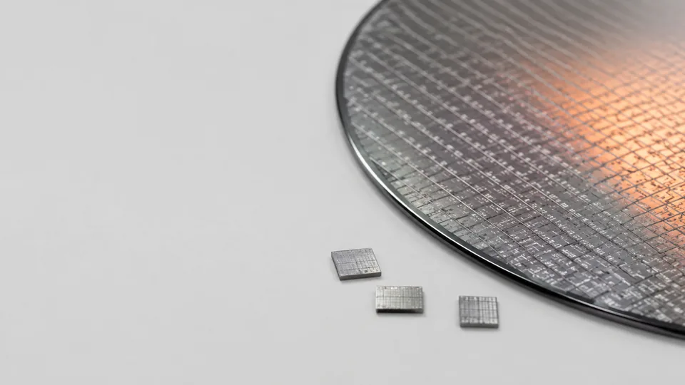
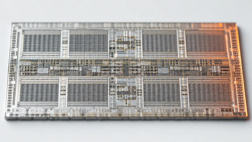
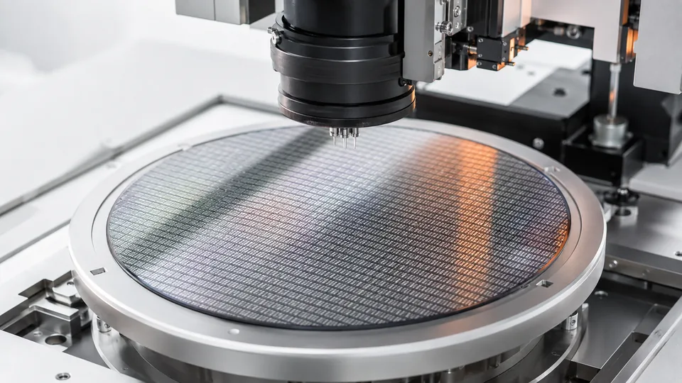
The HC1 is the first chip from Taalas, announced in February 2026. Instead of loading a model into memory and running it on general-purpose hardware, it has one model, Llama 3.1 8B, built into the chip itself. This approach is called model-on-chip, or a hardwired LLM.
Fanshi Semiconductor is not affiliated with Taalas. This page summarizes what has been published, with sources at the end, because the HC1 is the clearest public reference point for the approach.
Published figures
| Item | Published figure | Reported by |
|---|---|---|
| Model | Llama 3.1 8B, hardwired | Taalas, via CNX Software and heise |
| Speed | Close to 17,000 tokens/s per user | Vendor-reported |
| Process | TSMC 6 nm | CNX Software, heise |
| Die size | 815 mm² | CNX Software, heise |
| Transistors | About 53 billion | CNX Software, heise |
| Precision | 3-bit and 6-bit parameters in the first silicon | Taalas, via heise |
| Flexibility | LoRA adapters and a configurable context size | CNX Software |
| Deployment | Servers of around 2.5 kW | CNX Software |
| Same model on NVIDIA H200 | About 230 tokens/s per user | Nvidia baseline, cited by heise |
| Same model on Cerebras | About 1,900 tokens/s | Artificial Analysis, cited by heise |
| Same model on Groq | About 600 tokens/s | Artificial Analysis, cited by heise |
Figures are as published during 2026. The HC1 speed is a vendor figure; the Cerebras and Groq figures come from an independent tracker.
Where the speed comes from
Generating one token requires every weight in the model. On a GPU the weights sit in memory and have to be fetched for each token, so the limit is how fast memory can deliver them. The HC1 removes the fetch: the weights are part of the circuit, so there is nothing to move.
That is why the gain is so large for a small model. An 8B model is not compute-bound on modern hardware; it is bound by the movement of data. Take away the movement and the same arithmetic runs tens of times faster.
The limits
- One model per chip. A different model means a different chip. Adapters and context size can be configured, the base weights cannot.
- Quantization. By the company's own account the first silicon uses 3-bit and 6-bit parameters, which costs some quality against a GPU baseline.
- Vendor figures. The headline speed is reported by the company. Check for independent measurements before relying on it.
- It is a data-centre part. Servers of around 2.5 kW do not go inside a product.
What it means for devices
The HC1 shows that fixing the weights in place works at scale. It does not solve the device problem, because a translator, a vehicle module or a robot has one watt to a few tens of watts, not kilowatts, and a bill of materials that cannot absorb a leading-edge chip of that size.
Edge chips apply the same principle with different constraints: smaller models, mature process nodes and three ways of holding the weights. MaskROM compute-in-memory fixes them at manufacture, SRAM compute-in-memory loads them at power-up, and near-memory compute keeps them in external memory where they can be updated.
Fanshi builds chips of this kind on SMIC 28 nm. Its published figures are design targets, not measurements: Forge targets 17,000 token/s on Qwen 3.5 0.8B in a watt-class device, and Trident targets 15,000 token/s on models up to Qwen 3.5 35B within a 70 W system budget.
Frequently asked questions
What is the Taalas HC1?
A data-centre inference chip, announced in February 2026, with the Llama 3.1 8B model hardwired into the silicon. The company reports close to 17,000 tokens per second per user.
How fast is the Taalas HC1 compared with a GPU?
Taalas reports close to 17,000 tokens per second per user on Llama 3.1 8B. Press coverage cites roughly 230 tokens per second per user for the same model on an NVIDIA H200. The HC1 figure is vendor-reported.
Can the Taalas HC1 run other models?
No. The base model is fixed in the chip. According to press coverage it supports LoRA adapters and a configurable context size, but a different base model requires a different chip.
Can the Taalas HC1 be used in an edge device?
No. It is designed for servers of around 2.5 kW. Devices use edge inference chips built on compute-in-memory or near-memory compute, which target one watt to a few tens of watts.
Is Fanshi affiliated with Taalas?
No. Fanshi Semiconductor has no affiliation or partnership with Taalas. Taalas builds data-centre accelerators; Fanshi builds chips and IP for edge devices.